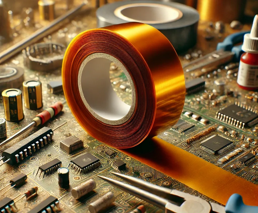
The Role of UV Curable Tapes in LED Production
In the fast-evolving world of LED manufacturing, precision is everything. Whether producing standard LEDs, miniLEDs, or microLEDs, the integrity of each chip matters. During wafer dicing, back grinding, and chip separation, manufacturers use UV curable tape to hold delicate substrates securely.
This tape provides strong temporary adhesion to prevent shifting, cracking, or flying chips during high-speed processing. Once exposure to UV light occurs, the adhesive weakens significantly, allowing for a clean, residue-free release—preserving both the chip and the tool.
How UV Curable Tapes Work
The functionality of UV curable tape is based on photo-reactive adhesive technology:
- Before UV exposure: The adhesive maintains strong holding power, keeping wafers or chips firmly in place through cutting and grinding.
- After UV exposure: A brief dose of UV light (commonly 200–400 nm) disrupts the adhesive matrix, reducing peel strength drastically. This allows the tape to be removed cleanly without damaging delicate components.
This dual-stage behavior enables manufacturers to balance stability during processing and flexibility during removal.
Applications in LED Manufacturing
UV curable tapes are tailored for:
- LED chip cutting and separation
- miniLED and microLED frame processing
- High-resolution glass printing for display backplanes
- Die sorting and wafer-level packaging
These tapes are essential wherever precise alignment and safe removal are needed without residue contamination.
Key Benefits of UV Curable Tapes
UV tapes offer a reliable, efficient, and clean approach to chip handling. Their main advantages include:
- Damage Prevention: Avoid chip flying, corner breakage, or microcracks during dicing.
- Clean Removal: No residue left behind after UV exposure.
- Enhanced Yield: Supports tight tolerance assembly without rework.
- Environmental Durability: Resistant to shear, stress, and moisture in industrial settings.
- Multiple Thickness Options: Tailored for different wafer sizes, frames, and process depths.
Technical Features of UV Curable Tape for LED Manufacturing
| Feature | Specification |
|---|---|
| Adhesive Type | UV-curable acrylic |
| Base Film | Polyolefin |
| Initial Peel Strength | High |
| Post-UV Peel Strength | Very low |
| Available Thickness | 50 μm – 150 μm |
| UV Wavelength | 200–400 nm |
These parameters allow LED producers to tune the tape’s properties based on tool speed, chip size, and UV exposure setup.
Material Options: Polyolefin Base Film Performance
Polyolefin is a preferred base film material for UV tapes due to:
- Excellent shear strength: Prevents shifting during dicing.
- Chemical resistance: Withstands solvents used in post-process cleaning.
- Dimensional stability: Maintains structure under thermal and UV stress.
- Flexibility: Adapts to curved surfaces and varied wafer geometries.
UV Curable Tape vs. Thermal Release Tape
While both UV and thermal release tapes are used in semiconductor and LED processing, they serve different needs:
| Feature | UV Curable Tape | Thermal Release Tape |
|---|---|---|
| Release Method | UV exposure | Heat activation |
| Suitable For | LED chip cutting, wafer handling | Ceramic/MLCC dicing |
| Release Time | Immediate post-UV | Delayed post-heat |
| Adhesive Control | Optical trigger | Thermal control |
| Residue Risk | Very low | Low |
Choosing the Right UV Tape for LED Applications
Selecting the best UV curable tape involves:
- Thickness calibration: Thicker tapes protect deeper cuts; thinner for shallow work.
- UV dose compatibility: Ensure your UV lamps meet the required spectrum and exposure time.
- Surface compatibility: Match tape formulation with substrate materials such as glass, polyimide, or GaN.
Common Challenges Solved by UV Curable Tapes
- Chip misalignment: Strong initial adhesion keeps chips fixed during handling.
- Chipping and delamination: Elasticity absorbs shock during blade movement.
- Manual peeling damage: UV weakening ensures effortless removal without tools.
- Residue pollution: Controlled formulation avoids contamination, critical for display-grade LEDs.
FAQs About UV Curable Tape in LED Manufacturing
Q1: Can UV curable tape be reused?
No. These tapes are designed for single-use to ensure consistent adhesion and clean release.
Q2: What UV light is required?
A wavelength of 200–400 nm is standard, with 365 nm commonly used in industrial setups.
Q3: Is it compatible with microLED production?
Yes. The tape’s high precision and clean release make it ideal for small die sizes and tight layouts.
Q4: Will it affect chip yield?
No. In fact, using UV curable tape improves yield by reducing handling defects and contamination.
Q5: How long can it be stored?
Most products offer a shelf life of 6–12 months under cool, dry conditions.
Q6: Is the tape RoHS compliant?
Yes. High-quality UV tapes meet RoHS and related environmental standards.
Conclusion: Clean Release Solutions for High-Yield LED Manufacturing
As LED technology advances, so does the demand for clean, reliable, and efficient processing materials. UV curable tapes offer strong wafer support during fabrication and effortless removal after UV exposure—supporting higher yields and less waste.
For LED manufacturers seeking robust, high-performance solutions, Fonitaniya provides UV curable tape engineered specifically for modern miniLED and microLED processes.